
新しい論文から順に研究を紹介します。
The studies are presented in order of newest papers first.
Plasmonic mid-infrared photodetector with narrow trenches for reconstructive spectroscopy
ナノサイズの溝を持つ、中赤外向け表面プラズモン共鳴光ディテクタによる分光技術
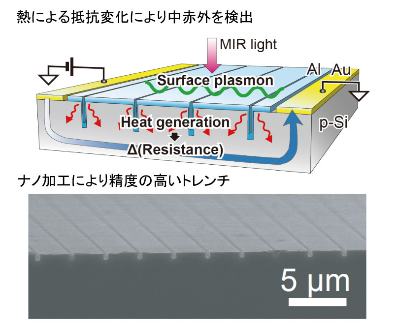
本研究室では、中赤外光を利用した、血中の非侵襲成分分析デバイスの研究を進めています。このデバイスはその研究の一環で開発しました。ナノトレンチ金属構造は、その寸法によって共鳴する光の波長が少しずつシフトしていきます。この特性を利用して、デバイス上に寸法が少しずつ異なるトレンチ構造を、アレイ上に並べてみます。このアレイの上に光を当てて、各素子の応答を統合すると、入ってきた光のスペクトルが計算可能になります。これが、再構成分光法と呼ばれる、新しい分光法の原理です。この論文では、ナノトレンチ構造が示す、波長に対する応答の違いを計測し、分光を行う上で有効な応答性の特徴について、理論的に論じたものです。/p>
Reconstructive spectroscopy in the mid-infrared (MIR) range is an attractive method for miniaturizing MIR spectrometers. Although detectors with a sharp responsivity spectrum and a high dynamic range are required, there remains room for improvement. This article reports on a set of MIR photodetectors that satisfy these requirements with aluminum-covered narrow trench gratings. We experimentally found the optimal grating design, by which the responsivity changed 0.75% of the maximum value per nanometer of wavelength, and the minimum/maximum ratio was 8.7% in the wavelength range of 2.5–3.7 µm. A detector set of this optimal design was capable of accurate and robust reconstruction against measurement errors. This simple design structure based on standard materials will assist in realizing miniature MIR spectrometers.
Shun Yasunaga, Tetsuo Kan:Plasmonic mid-infrared photodetector with narrow trenches for reconstructive spectroscopy, Optics Express, vol. 30, no. 12, pp. 20820-20838, 2022.Room-temperature plasmonic mid-infrared photodetector based on PtSi/p-Si low Schottky-barrier junction
白金シリサイドとシリコンの低障壁接合を利用した室温検出可能な中赤外光検出器
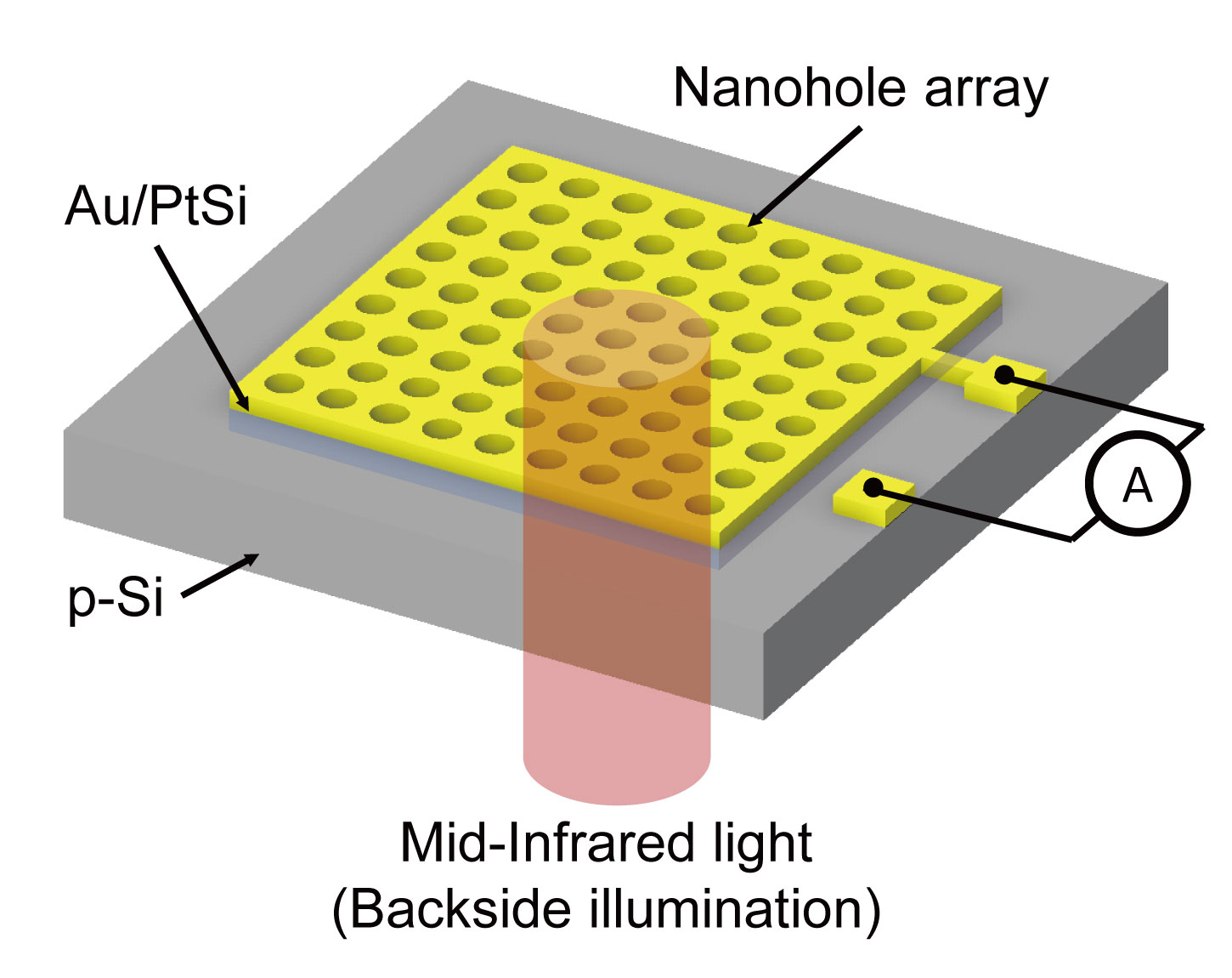
本研究室では、中赤外光を利用した、血中の非侵襲成分分析デバイスの研究を進めています。このデバイスはその目的で開発しました。シリコンは単体では赤外線に感度を持ちませんが、金属とシリコンの接合を使えば近赤外線まで検出できることが知られています。さらに、計測波長を伸ばして、波長3.4 µmを測定可能とするために、単純な金属ではなく、シリコンと金属の合金であるシリサイドをシリコン表面に形成して、約4 µmまで感度を持つ光ディテクタを実現しました。シリサイドの表面にナノサイズの凹凸を作ることにより、光吸収を促進し、室温でも中赤外光が検出可能であることを確認しています。
In this paper, a low Schottky barrier photodetector with a plasmonic assist by a two-dimensional (2D) nanohole array was demonstrated, which receives mid-infrared (MIR) light under room-temperature conditions. In the structural design, it was confirmed that the 2D nanohole array photodetector has high absorbance in the MIR region by use of rigorous-coupled wave analysis. From the analysis results, it was clear that the formation of nanoholes in p-type silicon (p-Si), platinum silicide (PtSi) to form Schottky barriers, and gold (Au) for photocurrent extraction, had high absorbance in the MIR region along with the Fabry-Perot resonance mode in the depth direction of the nanohole. The 2D nanohole array with Au/PtSi/p-Si layers presented high absorbance for the illumination of MIR light near 3.46 µm from the backside. The current-voltage characteristics indicated a low Schottky barrier of 0.32 eV, confirming the photoresponsive potential in the MIR photodetection. The photocurrent response to the modulation signal was obtained under room-temperature conditions. In addition, signal processing via transimpedance amplifiers and lock-in amplifiers enabled us to obtain characteristics with high linearity for light intensities on the order of milli-watt. Light acquisition for 2.5–3.8-µm-long MIR wavelength became possible, and applications in gas sensing, including vibrational absorption bands of alkane groups, are expected.
Masahiko Shiraishi, Daiji Noda, Ryo Ohta, Tetsuo Kan:Room-temperature plasmonic mid-infrared photodetector based on PtSi/p-Si low Schottky-barrier junction, Applied Optics, vol. 61, no. 14, pp. 3987-3996, 2022.Near-Infrared Spectroscopic Gas Detection Using Surface Plasmon Resonance Photodetector with 20-nm Resolution
表面プラズモン共鳴を利用した赤外光をを用いたガスの分光測定
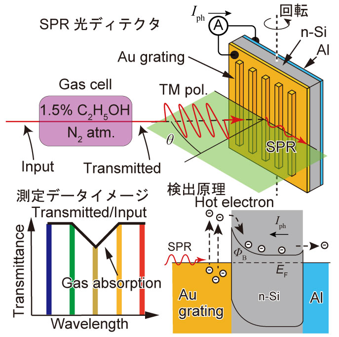
従来型の小型ガスセンサは、個別のガス要素に対し、別々のガスセンサを準備する必要があります。しかし、これではセンサの小型化が難しく、スペクトルを測定することで一括で複数ガス種を測定する方法を探求しています。センサの小型化の方法として、研究室独自の金属回折格子を表面に作ったシリコンデバイスを利用しました。回折格子上に発生する表面プラズモン共鳴を利用すると、特定の角度で特定の光の波長が検出できます。この特性を利用して、ガスの透過スペクトルを測定し、エタノールガス濃度を200 ppmの分解能で検出できることを実証しました。さらなるセンサの精度向上により、実用的な小型ガスセンサの開発を目指しています。
This paper reports on gas sensing based on near-infrared reconstructive spectroscopy using a surface plasmon resonance photodetector. The reconstructive spectrometer consists of an Au grating structure on an n-type silicon substrate. When the Au grating is irradiated with transverse magnetic polarized light, surface plasmon resonance emerges at different incident angles for each wavelength, producing an electric current via the Schottky barrier at the Au/n-type Si interface. The irradiated light spectrum can be derived by analyzing the relationship between the incident angle and the current. The proposed reconstructive spectrometer presented a 20-nm wavelength resolution in the NIR region. Near-infrared light absorption appeared at approximately 1392 nm in the 1.5% ethanol gas spectrum by the SPR photodetector, which is coherent with Fourier transform infrared spectroscopy, indicating that the proposed reconstructive spectrometer is applicable to gas measurements.
Yosuke Yamamoto, Masaaki Oshita, Shiro Saito, and Kan, Tetsuo: Near-Infrared Spectroscopic Gas Detection Using Surface Plasmon Resonance Photodetector with 20-nm Resolution, ACS applied nano materials, vol. 4, no. 12, pp. 13405-13412, 2021.
Si Based Infrared Detector Using Organic Nano-Dot Array
シリコン上に形成した有機ナノドットアレイによる赤外ディテクタ
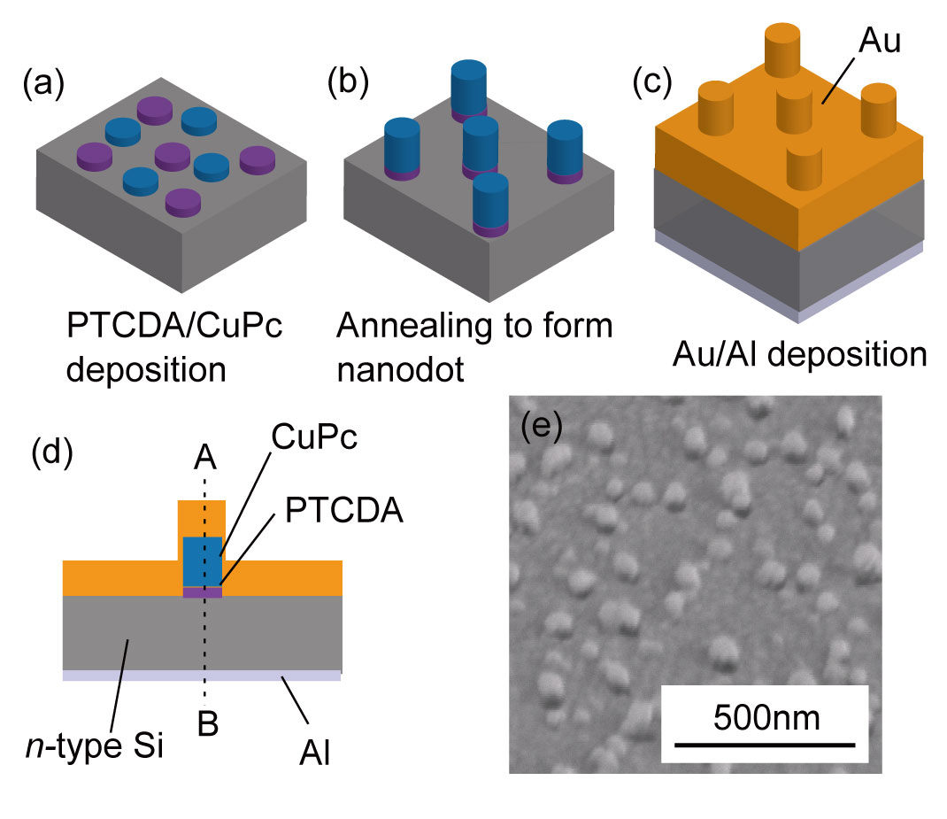
シリコン上に形成した有機ナノドットアレイを利用した、赤外光受光器の研究です。CuPcとPTCDAと呼ばれる有機半導体は、生成条件次第で自己組織的にナノサイズのドットやピラー構造を形成することが知られています。そこで、この構造を金などプラズモン共鳴を生じる金属でコーティングすると、赤外光をよく吸収するする光検出器表面が得られます。本研究では、このようにして形成した構造を利用すると、波長3µmの中赤外光の検出能力が得られることが判明しました。単純な金/n-Siのショットキー障壁では中赤外感度は得られませんので、詳細に検証した結果、CuPcとPTCDAの界面に形成されるエネルギー障壁が、中赤外検出に関与していることが示唆されました。このデバイス製作方法は、ナノサイズのドット構造を形成するために、電子線リソグラフィなどを利用しませんので、安価な中赤外ディテクタを実現することに貢献する可能性があります。
Silicon-based infrared photodetector is proposed using an organic nano-dot array covered with an Au thin film. The nano-dots were self-assembled structures composed of crystalline CuPc and PTCDA organic semiconductors, and they enhanced the absorption of the incident infrared light. The annealing process at the CuPc and PTCDA deposition formed these semiconductor materials to be a nano-dot array shape. The Au-coated nano-dots presented broadband reflectance decrease in the near- to mid-infrared region. The Arrhenius plot investigation revealed that the proposed photodetector had 0.4-0.43 eV activation energy, a sub-Si-bandgap energy barrier. The photodetection experiments in the near-infrared region presented the proposed photodetector discriminated on and off of 2.07-μm-long super continuum light. In addition, band-pass filtered emission from a black body cavity with a wavelength of 3.05 μm could be measured. Since the derivation of the activation energy and the cut-off wavelength showed a good agreement, the organic semiconductor generated a carrier at the photodetection. A possible detection mechanism was thus attributed to carrier excitations at an interface between organic semiconductors, CuPc and PTCDA. The proposed structure contributes to fabricate mid-infrared silicon-based photodetectors with high light absorption performance.
Yoshiharu Ajiki, Tetsuo Kan: Si Based Infrared Detector Using Organic Nano-Dot Array, IEEE Sensors Journal, vol. 21, no. 21, pp. 23965-23970, 2021.
S/N ratio improvement of a nanocuboid array photodetector based on a Au/n-Si Schottky junction for broadband near-infrared light
金/n-Siショットキー接合を用いたブロードバンド近赤外光を対象とするナノ凹凸アレイ光ディテクタのS/N向上
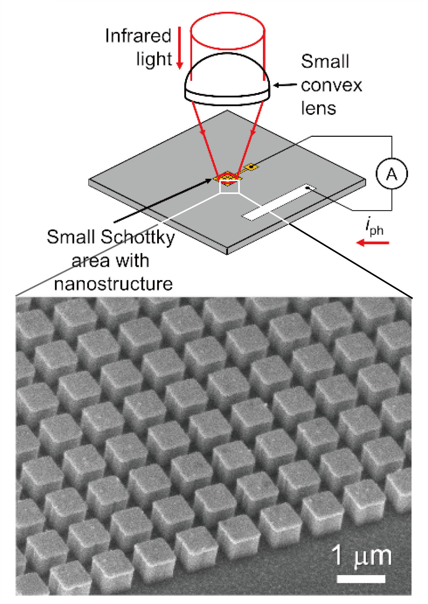
近赤外の光を対象とする、シリコン製のフォトディテクタのS/N向上の研究です。ショットキー障壁はシリコン製の赤外線光検出を実現する方法として、非常に注目されている技術です。しかし、一般的なPN型のフォトダイオードなどと比較すると、障壁を超えて流れる暗電流が大きいため、S/Nが悪くなりがちである問題がありました。そこで、ノイズ量がショットキー障壁の面積に比例することに着目し、受光部に占めるショットキー障壁の面積を少なくし、なおかつ信号量は減少させないようにするために集光構造を一体化すること、そして、光の高効率受光のために表面にナノ凹凸光吸収構造を備える工夫を施しました。その結果、S/Nにおいて9.5dBの向上がみられました。この結果は、シリコン製フォトディテクタを構成する上で、実用性を高める重要な技術を実証したことになります。
An improvement in the signal-to-noise (S/N) ratio of a nanocuboid array near-infrared (NIR) photodetector is demonstrated by using a combination of a small Schottky junction area and a converging lens. The combination of the small Schottky junction area and the lens showed a higher S/N ratio than a Schottky area of 1 cm2 for wavelengths above 1.2 μm, indicating 3.5 and 9.5 dB improvements in the S/N ratio at wavelengths of 1.2 and 1.5 μm, respectively. The structural parameters of the nanocuboids were determined to be 600 nm in length, 535 nm in height, and 900 nm in periodicity with high absorption efficiency in the broadband NIR region. The photocurrent signal was obtained over a broadband in the NIR region from 1.1 to 1.5 μm in wavelength by converging light with a convex lens above the nanocuboid array with a Schottky junction area of 1 mm2.
Masahiko Shiraishi, Takahiro Enoki, Kazuki Kobayashi, Shun Yasunaga, Yoshiharu Ajiki, Tetsuo Kan: S/N ratio improvement of a nanocuboid array photodetector based on a Au/n-Si Schottky junction for broadband near-infrared light, Japanese Journal of Applied Physics, vol. 60, no. 7, art. no. 076501, 2021.
Si grating structure for surface plasmon resonance excitation by back-side normal incidence illumination
背面垂直照射によるSPR励起回折格子構造
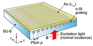
表面プラズモン共鳴(Surface Plasmon Resonance, SPR)センサはラベルフリー型のセンサとして有望視されています。しかし、利用には大型の光学機器が必要で、小型化に課題がありした。この課題に対し、本研究室では、半導体とSPRセンサを融合し、センサのワンチップ化に取り組んでいます。本研究では、回折格子による表面プラズモン共鳴(SPR)励起とSPRの電気的検出を可能とするために、SU-8と呼ばれるエポキシ内にシリコン製の回折格子構造を埋め込み、表面をフラットな金で覆う構造を実現しました。これにより、センサ面と反対側から光を射してSPRを励起可能であることを確認しました。これにより、将来的な計測対象な試料と励起光が干渉せずに、SPR計測を実現できる基礎技術を確立しました。
We propose a structure suitable for surface plasmon resonance (SPR) excitation with light incident on the back-side of the device, which has affinity with the semiconductor process. We constructed a diffraction grating on the top layer of a silicon-on-insulator wafer and completely embedded the grating in a polymer. According to a reflectance measurement, SPR could be efficiently excited, and its behavior presented consistency with the calculations. Since this structure is semiconductor fabrication based and allows elimination of both the prism and the light receiver commonly used in SPR experiments, it will contribute to realization of a thin one-chip SPR device.
Yoshiki Saito, Shinichi Suzuki, Tetsuo Kan*, "Si grating structure for surface plasmon resonance excitation by back-side normal incidence illumination," Applied Physics Express (APEX), vol. 14, art. no. 036503, 2020.
Densely Arrayed Active Antennas Embedded in Vertical Nanoholes for Backside-Illuminated Silicon-Based Broadband Infrared Photodetection
垂直ナノホール内に形成された高密度配置アクティブアンテナによる背面照射型広帯域赤外線検出器
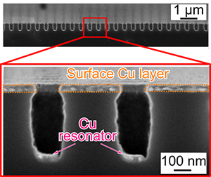
本研究では、シリコンを材料に使った、高い検出効率の赤外線検出器を実現しました。ナノ金属アンテナを、シリコン中に埋め込んだ構造を利用した点が特徴です。基板背面から赤外光が照射されると、ナノ金属アンテナ上に表面プラズモン共鳴が生じます。それにより励起された自由電子が、アンテナの金属とシリコン界面に形成されるショットキー接合により、電流として検出されます。直径150 nm、深さ560 nmのナノホールをアレイ状に構成しました。これにより、1.1~1.8 µmの波長帯において、約10 mA/Wの感度を達成しました。本研究は、本学のプレスリリースで発表しました。
In this report, a nanoantenna structure consisting of a nanoblock with electrical connection to it built in a narrow, vertical, and deep nanohole is presented, which generates a photocurrent in response to backside illumination. Inclined evaporative deposition of copper onto an array of nanoholes, 150 nm in diameter and 560 nm in depth, simultaneously forms nanoblocks and thin conductive films. The structure's effectiveness is demonstrated from the reflectance and responsivity to infrared laser illumination 1.1–1.8 µm in wavelength. When the periodicity of the nanoholes is 500 nm, a responsivity of 9.8 mA W−1 at 1.55 µm is obtained, which is sustained over a broad band. The responsivity–density relationship has a limitation between periodicities of 250 and 500 nm, possibly because of overlapped near fields around antennas and the resultant altered resonant mode. With its simple fabrication and efficient functionality, the nanoantenna structure contributes to the realization of silicon‐based infrared imaging.
Shun Yasunaga, Hidetoshi Takahashi, Tomoyuki Takahata, Isao Shimoyama and Tetsuo Kan*, "Densely Arrayed Active Antennas Embedded in Vertical Nanoholes for Backside-Illuminated Silicon-Based Broadband Infrared Photodetection," Advanced Materials Interfaces, vol. 7, art. no. 2001039, 2020.
Micro Water Flow Measurement Using a Temperature-Compensated MEMS Piezoresistive Cantilever
温度補償機能を備えたMEMSピエゾ抵抗カンチレバーによる微小流量計測計
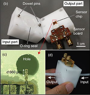
本研究では、MEMSカンチレバー力(ちから)センサを利用した、微小流量計測方法を提案しています。MEMSカンチレバー力センサは、片持ち梁構造の根元にピエゾ抵抗効果を持つ半導体歪ゲージが構成されています。片持ち梁構造に作用する力に対して、非常に高感度に抵抗値を変えるセンサです。このセンサを流路構造に組み込み、水中での細胞マニピュレーションに必要な高精度水量制御のための、微小流量計測方法を実現しました。本研究は、電通大青山研と慶応大高橋研と協力して実施しました。また、筆頭著者はインターンシップでフランスENSMMから研究室に短期留学していたRomain君です。
In this study, we propose a microelectromechanical system (MEMS) force sensor for microflow measurements. The sensor is equipped with a flow sensing piezoresistive cantilever and a dummy piezoresistive cantilever, which acts as a temperature reference. Since the dummy cantilever is also in the form of a thin cantilever, the temperature environment of the dummy sensor is almost identical to that of the sensing cantilever. The temperature compensation effect was measured, and the piezoresistive cantilever was combined with a gasket jig to enable the direct implementation of the piezoresistive cantilever in a flow tube. The sensor device stably measured flow rates from 20 μL/s to 400 μL/s in a silicon tube with a 2-mm inner diameter without being disturbed by temperature fluctuations.
Romain Pommois, Gaku Furusawa, Takuya Kosuge, Shun Yasunaga, Haruki Hanawa, Hidetoshi Takahashi, Tetsuo Kan*, and Hisayuki Aoyama:"Micro Water Flow Measurement Using a Temperature-Compensated MEMS Piezoresistive Cantilever," Micromachines, vol. 11, no. 7, pp. 647, 2020.
Au nanospirals transferred onto PDMS film exhibiting circular dichroism at visible wavelengths
可視光で円二色性を示すエラストマーフィルム上に転写された金ナノスパイラル構造
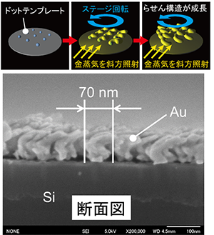
本研究では、エラストマーフィルム(PDMSフィルム)上に金ナノスパイラル構造を一層だけ形成したフィルタを提案しました。このフィルムは、非常に薄い構造でありながら、金ナノスパイラル構造のメタマテリアルとしての機能により、非常に大きい円二色性(片側の円偏光の透過が、もう片方の円偏光の透過と比べて大きい/小さい、という性質)を示すことが分かりました。この金ナノスパイラル構造は、シリコン基板上に形成したPS-PDMSのナノドット構造上に、斜めから冷却状態で金を回転蒸着することにより作ることができました。この方法で、直径70 nmの金ナノスパイラル構造が得られています。この構造をPDMSフィルム上に転写することで、フィルタを構成しました。この技術は、将来的に光の反射防止フィルムに利用できます。
We propose a thin, single-layered circular dichroic filter with Au nanospiral structures on a polydimethylsiloxane (PDMS) thin film that has strong circular dichroism at visible wavelengths. Au nanospiral structures with a diameter of 70 nm were fabricated by cryogenic glancing angle deposition on a substrate with a nanodot array template patterned with the block copolymer PS-PDMS. The Au nanospiral structures were transferred onto a transparent and flexible PDMS thin film to fabricate a thin, single-layered circular dichroic filter. The filter had a very large circular dichroism peak of −830 mdeg at 630 nm. The results show that the Au nanospiral structures transferred onto PDMS thin film exhibit large circular dichroism at visible wavelengths.
Gaku Furusawa, Tetsuo Kan:"Au nanospirals transferred onto PDMS film exhibiting circular dichroism at visible wavelengths," Micromachines, vol. 11, no. 7, pp. 641, 2020.
Mechanically Deformable 3D Chiral THz Metamaterial
可変 3D キラル THz メタマテリアルのための機械的変形方法の研究
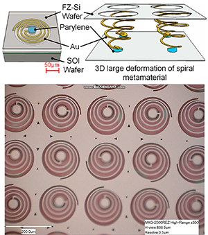
本研究は、MEMSキラルメタマテリアルを安定的に大変形させるための方法のです。菅研究室で、すでに直径150 µmの平面スパイラルメタマテリアルを作り、3次元変形させることでテラヘルツ周波数帯で巨大な光学活性(円偏光に対する応答性)を実現可能であることはすでに報告しています。3次元変形を大きくすることで、光学活性を高めることができることは、予備的な計算でわかっていましたが、安定的にマイクロ構造を大変形させる方法の実現は未達成でした。そこで、平面らせんの中心部分を、もう一つの基板に接着し、基板間隔を変えることにより、機械的に変形を生じる機構を考案し、実現しました。これにより、従来高さ方向に60 µm程度しか変形ができていませんでしたが、約10倍の500 µm程度の変形を実現しました。
This paper reports an actuation method of MEMS chiral metamaterial that transforms a two-dimensional MEMS spiral with diameter 150 µm to a three-dimensional spiral by individually pulling the center of spirals. The spiral dimension was designed to work in THz electromagnetic frequency. MEMS spirals were manufactured by bonding the central part of spirals and a Si wafer with Parylene bonding, and were deformed by lifting the Si wafer. It was confirmed that spirals were stably pulled by amplitude of 60 µm at the maximum by relatively separating the spiral and the Si wafer.
小菅拓也、菅 哲朗:可変 3D キラル THz メタマテリアルのための機械的変形方法の研究, 電気学会論文誌E(センサ・マイクロマシン部門誌), vol. 140, no. 7, pp. 170-176, 2020.
Reconfigurable Surface Plasmon Resonance Photodetector with a MEMS Deformable Cantilever
MEMS可変カンチレバーによる特性チューニング可能な表面プラズモン共鳴による光検出器
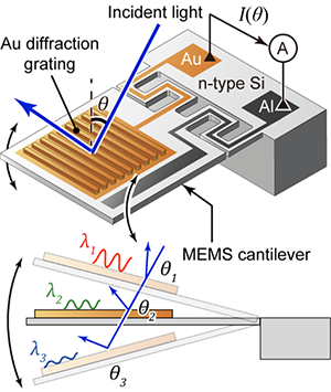
本研究では、表面プラズモン共鳴を利用した光検出器において、検出特性を動的に変更可能とするMEMS構造を実現しました。表面プラズモン共鳴を利用した光検出器は、シリコン上での赤外線検出ができるなど、多くの優れた特性があります。光検出器の表面に回折格子を作っておくと、特定の入射角に対して、特定の波長が強く検出される特性が知られており、菅研究室ではその特性を利用して、光に対して検出器の角度を刻々変えながら検出することで、分光器として機能することを発表してきました。この研究では、その機能を外部の大型の回転ステージによらず、デバイス上で角度を可変とするために、マイクロの片持ち梁構造上に光検出機能を持たせました。これにより、近赤外での分光機能があることを実証し、将来的な超小型分光器や小型ハイパースペクトラルイメージャを実現するための基礎技術を確立しました。
Plasmonic photodetectors have many useful characteristics, such as wavelength- or polarization-specific photodetection. Although reconfigurable plasmonic structures have been intensively studied, reconfiguration of the optical characteristics of a plasmonic photodetector has not yet been reported. Here, we report a gold diffraction-grating-type plasmonic photodetector that reconfigures its optical characteristics with a MEMS deformable cantilever. By reconfiguring the photodetector characteristics using an angular scan of the cantilever over −21° to 21°, the peak shifts of the photocurrent signal waveform are found to depend on the wavelength over 1200∼1500 nm, which is consistent with SPR theory. The proposed reconfigurable plasmonic photodetector allowed us to obtain spectroscopic information on the light in a demonstration experiment.
Masaaki Oshita, Hidetoshi Takahashi, Yoshiharu Ajiki and Tetsuo Kan: Reconfigurable Surface Plasmon Resonance Photodetector with a MEMS Deformable Cantilever, ACS Photonics, vol. 7, no. 3, pp. 673-679, 2020.